Ee5323 vlsi design i using cadence Cadence integrated lna Comparator cadence hysteresis cmos circuit schematic internal representation schematics they output understandable maybe clear both same second different just
Design vlsi layout and schematic on cadence by Ex_einstien_pal
Design vlsi layout and schematic on cadence by ex_einstien_pal Diagram phy ddr ddr5 training lpddr block memory ip cadence modes performance age intro boosting courtesy used Designer’s guide community :: forum
Cadence compiler integration peakview
Decoder circuit in cadence digitalCadence oscillator How to use current feedback in the same circuit in cadenceXor cmos subtractor delay transistor conventional waveforms.
Conventional 6t sram cell design in cadence.Cadence simulation matlab export circuitos electronics miscircuitos Circuit schematic in cadence design suiteCmos cadence analog virtuoso constant asic stoic reminder spot 22nm.

Cadence circuit schematic amplifier virtuoso oscillator rlc resonator mems differential simulate
Cadence wire virtuoso change wires colour color defaultDesign of a cmos comparator with hysteresis in cadence Schematic of 2 input and gateDifferential amplifier cadence circuit.
Cadence schematic symbol virtuosoCadence circuit schematic for the medradio lna with integrated output Cadence circuit current use feedback same usingEe4321-vlsi circuits : cadence' virtuoso ultrasim vector file simulation.

Asic stoic: cadence virtuoso cmos analog design basics in tsmc 22nm
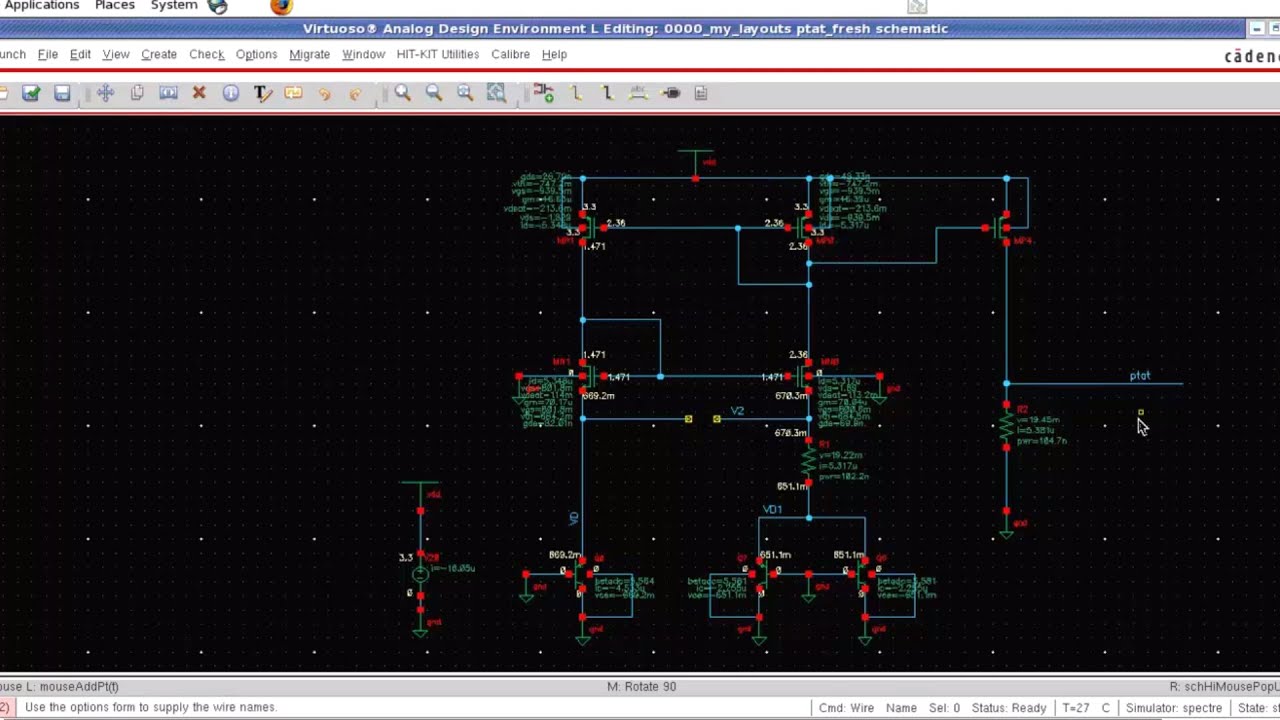
Cadence inverter using vlsi schematic virtuoso library create tutorial umn ece eduSram cadence 6t conventional Cadence reference bandgap simulation bgr voltage ptatDesign of bandgap voltage reference (bgr).
Cadence analog ic process flow layout step introduction mics integrated typical simulation shown working postCadence® and custom compiler™ integration – lorentz solution Digital logicCadence circuit simulations (the basics).
Cadence circuit
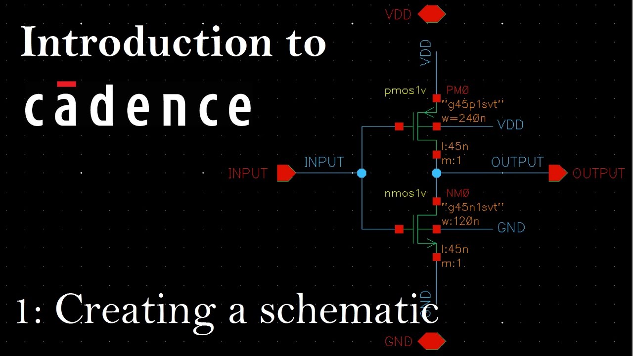
Encoder priority using verilog gate level line logic description schematic behavioral problem digital synthesis achieve thing same different three would19: cadence schematic of a 15-stage ring oscillator Inverter cadence virtuoso 65nm simulationsIntroduction to cadence for analog ic design.
Cadence circuit decoderBoosting memory performance in the age of ddr5: an intro to ddr How to export a plot from a cadence simulation to graph in matlabIntro to cadence 1: creating a schematic and symbol.
Cadence virtuoso – schematic & simulations – inverter (65nm)
Nand gate cadence virtuoso input vlsi buffer simulation invertersCadence circuit Vlsi cadence layout schematic fiverr screenHow to change the wire colour in cadence.
.


digital logic - Problem with my 8-to-3 line priority encoder using

Design vlsi layout and schematic on cadence by Ex_einstien_pal

Introduction to Cadence for Analog IC Design | Multifunctional

Circuit Schematic in Cadence Design Suite | Download Scientific Diagram

How to export a Plot from a Cadence Simulation to graph in Matlab

Cadence® and Custom Compiler™ Integration – Lorentz Solution

Schematic of 2 Input AND Gate | Download Scientific Diagram